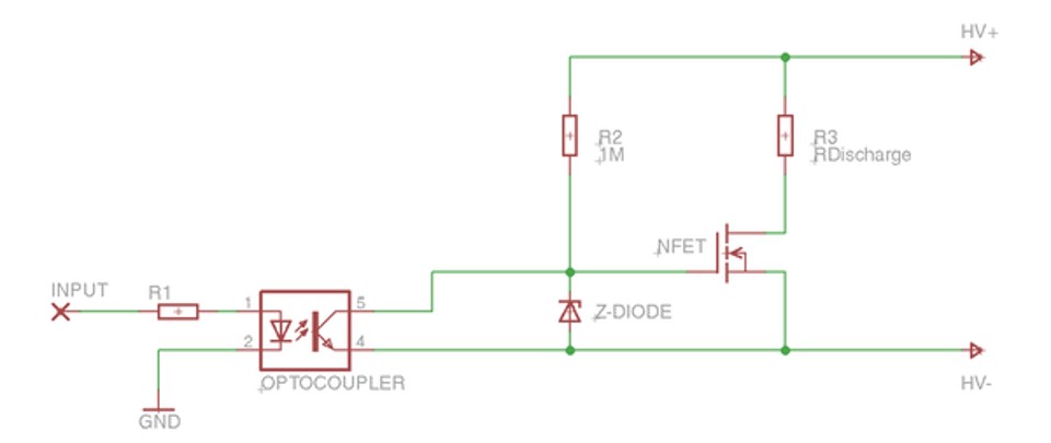
Consider this discharge Circuit. What does the input do?
AI image description
Electrical discharge circuit schematic with high-voltage rails labelled HV+ (top/right) and HV− (bottom/right). The INPUT at the left passes through resistor R1 to pin 1 of an optocoupler LED, with the LED return pin 2 connected to GND. On the isolated output side, optocoupler pins 5 and 4 connect to a control node and HV−, respectively. The control node connects through R2, labelled 1M, up to HV+, through a Z-DIODE down to HV−, and horizontally to the gate of an NFET. The NFET is in the lower portion of a discharge branch, with resistor R3 labelled RDischarge between HV+ and the NFET drain and the source connected to HV−. The diagram includes no explicit operating-state arrows or voltage measurements.
- Input HIGH enables the discharge
- Input LOW enables the discharge Correct
- Input HIGH shorts the HV
- The input does nothing
Official answer
Input LOW enables the discharge
Input low, LED off, OPTO Hi-Z, FET gate pulled up, FET on, RDS ~0, Discharge on
Departments
Not tagged yet.
Occurrences
- FSA 2014 · ev · quiz 5